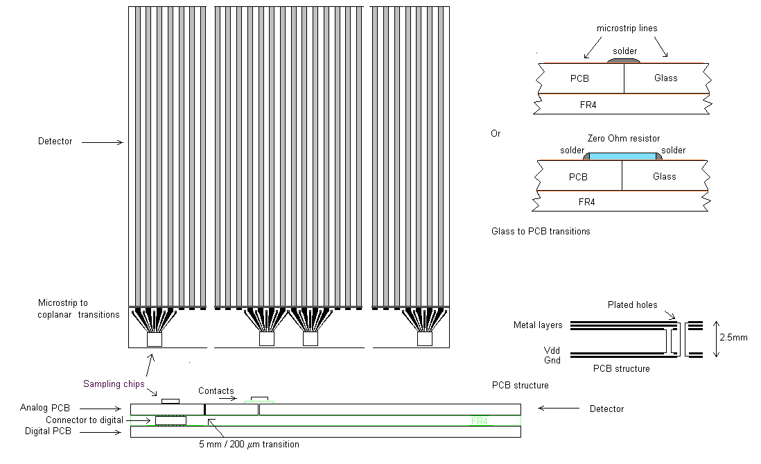
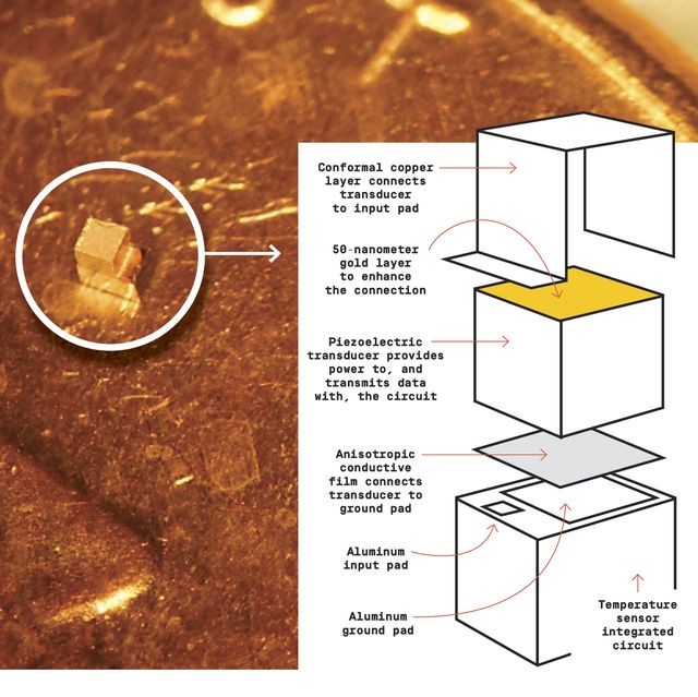
Details of TSFC bonding interfaces: tool/chip and bump/pad
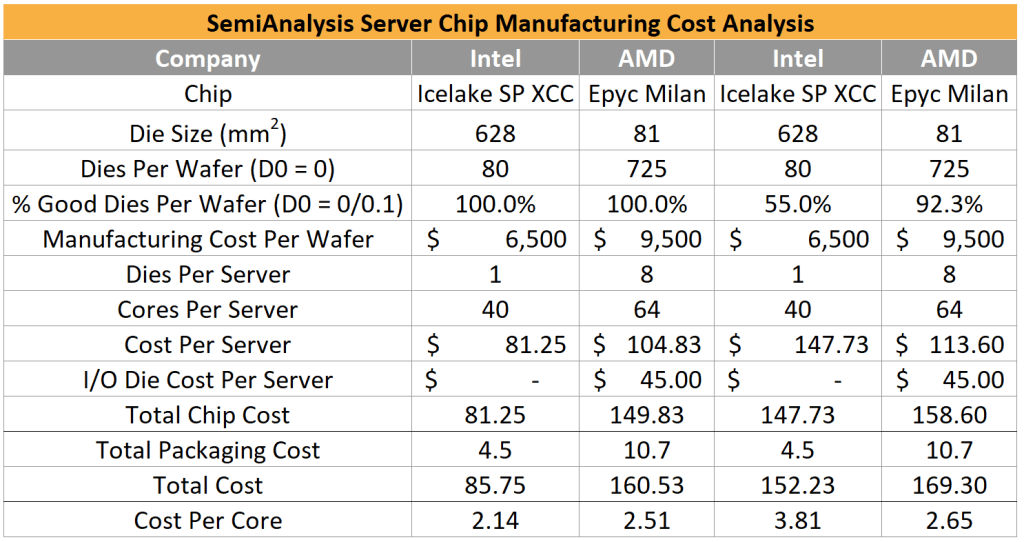
Advanced Packaging Part 1 – Pad Limited Designs, Breakdown Of Economic Semiconductor Scaling, Heterogeneous Compute, and Chiplets
Colour Sanitary Napkin Cold Mint Herbal Sanitary Pad Anion Chip
Repair damaged BGA chip pad
Wire bonding from chip to bonding pads and connection to leadframe.
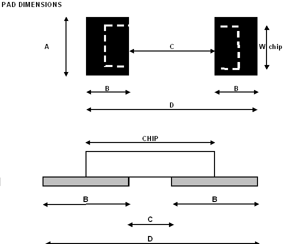
Details of test chip designs: pad pitch, layout, materials, and opening.
Chip Design
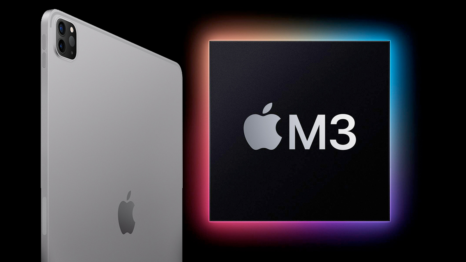
Next iPad Pro could skip straight to M3 Pro chip - Dexerto
Restored 2021 Apple 12.9-inch iPad Pro M1 Chip Wi-Fi 128GB - Space Gray (5th Gen) (Refurbished)
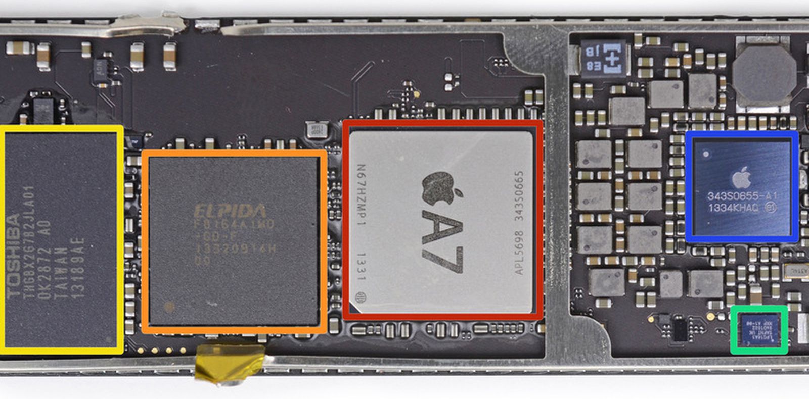
Teardown of iPad Air Reveals A7 Chip, LG Display, Qualcomm LTE Modem - MacRumors
Raspberry Pi 5 Active Cooler thermal pad alignment - Raspberry Pi Forums
Fermion: Monochrome OLED Display with Chip Pad - DFRobot
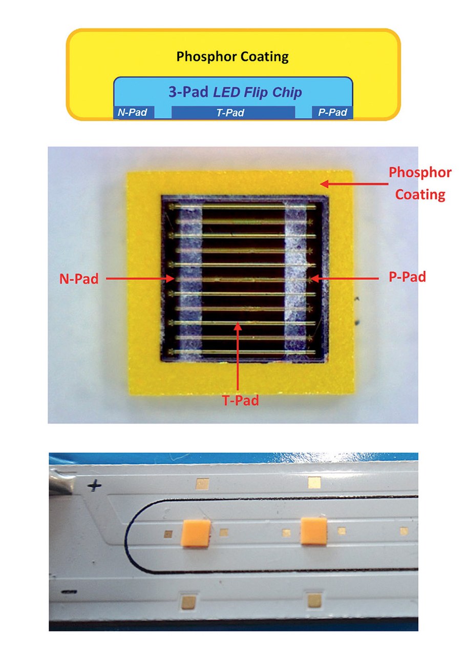
3-Pad LED Flip Chip COB — LED professional - LED Lighting Technology, Application Magazine
White Inkjet Printer Waste Ink Pad With Chip, For Printing Industry at Rs 300/pack in Mumbai
Touch of Lime - Garden of Eatin
Zulki's PCB Nuggets: What's Different Between C2 and C4 for PCB Microelectronics Assembly? :: I-Connect007
Anion Sanitary Napkins Sanitary Pad Ultra Thin
World's Smallest Implantable Chip
Outus 30 Pieces 2.6 x 0.8 Inch Silicone Thermal Pad Reusable Thermal Conductive Silicone Pad Each Thick for Gpu Heatsink CPU Chip Heat Conduction or
Pad Layout - Johanson Technology
PDF] Design and Fabrication of Bond Pads for Flip-Chip Bonding of
Schematic of the chip/bump build-up cross-section.
Chip Pad Bra Insert
Sensors, Free Full-Text